 Home >
 Knowledge Base >
 FAQs >
 Downloads >
FPGA based Resolver Conversion with Delta Sigma Technology
Valid for S700
Introduction
High performance servo drives are still a fast growing market segment. Resolvers are commonly used motor position sensing devices, fig. 1. Also, most modern controllers derive velocity feedback from the position sensor. The Resolver is an electromagnetic, rotational device that detects angular displacement. An equivalent electrical representation and diagram of typical output signal formats are shown in fig. 2. An ac excitation signal applied to the primary (rotor, ref) is inductively coupled to the two secondary (stator, sin and cosine). The transformation ratios are amplitude modulated by the sine and cosine of the angle of the rotor relative to the stator, θ.
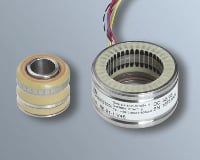
Fig. 1: Size 21 Resolver (LTN)
Due to the transformation principle an ac excitation or reference signal is necessary:
![]() (1)
(1)
The carrier frequency fC is always a compromise. To achieve low delay times with the conversion system a relatively high frequency is helpful. Regarding to long cables and the mechanical Resolver construction the carrier frequency is limited. Most Resolver data sheets are recommending a carrier frequency of 5 to 10 kHz. In servo drive applications this frequency is very often linked to the power stage switching frequency and the servo loop update rate.
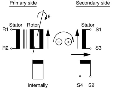
Fig. 2: Electrical representation of a resolver
The Kollmorgen Servostar product line is operating the Resolver with an 8 kHz carrier frequency {1}.
Resolver to Digital Conversion (RDC)

Fig. 3: Typical Resolver output signal formats
Input signals for the angle calculation are the two voltages from the secondary windings, fig 3:
![]() (2)
(2)
![]() (3)
(3)
The calculation is by theory just the solution of a simple equation with one division and an additional arc tan calculation
![]() (4)
(4)
The implementation is a bit more complicated. Executing a division and an arc tan is not trivial in an embedded system and especially in the moment where the signals (due to the carrier) are identical zero equation (4) is not applicable.According to these limitations the most common algorithm is utilizing a tracking control loop.
The math is based on the following trigonometrical relation:
![]() (5)
(5)
Replacing A with the real rotor angle θ and B with the negative estimated rotor angle ![]() we get:
we get:
![]() (6)
(6)
Defining the estimation error
![]()
and using a Taylor approximation around zero
![]()
we get:
![]()
or
![]() (8)
(8)
With demodulation of the carrier signal:
![]() (9)
(9)
![]() (10)
(10)
This is the fundamental math for the Resolver tracking algorithm, fig 4.

Fig. 4: Resolver tracking loop
The resulting transfer function of this tracking loop is:
 (11)
(11)
The bandwidth ![]() and the damping δ depend on the two parameters of the PI controller. Usually the bandwidth is set to a value in the area of 1000 Hz and the system is weakly damped, δ = 0.5.
and the damping δ depend on the two parameters of the PI controller. Usually the bandwidth is set to a value in the area of 1000 Hz and the system is weakly damped, δ = 0.5.
Key advantages of the tracking algorithms are:
- The conversion system needs only a sine and cosine function instead of the division and the arc tan functionality.
- A second order noise suppressing filter is “built in”
Special RDC Integrated Circuits
The traditional approach is to use an integrated resolver-to-digital conversion chip. Analog Devices for example offers some dedicated RDC-chips.
The Analog Devices 2S82 product is a complete 12 to 16-bit resolution tracking resolver-to-digital converter. The converter chip accepts 2V rms ±10% analog input signals on the SIN, COS and REF inputs. A type II control loop is employed to track the inputs and convert the input SIN and COS information into a digital representation of the rotor angle θ. By selecting external resistor and capacitor values the user can determine bandwidth, maximum tracking rate and velocity scaling of the converter to match the system requirements {2}.
By using such a dedicated RDC chip the servo drive design engineer gets a proved ready to use solution with well known specifications.
The disadvantages of dedicated circuits are:
- high cost for the RDC chip
- additional PCB-space
- limited performance: the design has to be optimized for high motor speed or for high resolution
- limited flexibility: fixed tracking loop bandwidth, no sin/cos gain mismatch compensation
- phase lag due to the tracking loop (depends on the tracking loop bandwidth)
Due to the fact that disadvantages prevail most modern servo drives are not using a dedicated RDC-chip. Modern drives are usually designed with a Field Programmable Gate Array (FPGA) area or CPU resources reserved for feedback processing. This logic configuration area is designed flexible for several feedback interfaces.
Software Resolver to Digital Converter
Analog-to-digital converters with multiplexed inputs are often used in digital servo drives {3}. The reference signal VREF (ideal sine) is generated by higher order filtering of a digital (rectangular) signal. The secondary signals VSIN and VCOS are sampled with two available channels typically at least at the maximum (2πfCt = π /2) and at the minimum (2πfCt = 3π /2) of the reference signal. Due to the max, min sampling the carrier demodulation is just a sign modification:
![]() (12)
(12)
The update rate of this digital tracking loop is two times the Resolver reference frequency:
![]() (13)
(13)
The tracking loop is usually realized with digital signal processing algorithms in a real time task of the drive microcontroller (software).
To achieve a RDC bandwidth of more than 1 kHz with an acceptable signal to noise ratio the analog Resolver signals need special filtering. Using 2nd order low pass filters or a band pass filter is common. Drawback of these higher order filters is the phase lag. Even by using low tolerance components for the production process the carrier signal phase lag can change significantly from drive to drive.
Using 12-bit sampling analog-to-digital converters and Gaussian error distribution the rotor angle can get a precision of up to 14.5 bit per revolution.The additional 2.5 bits are resulting from the arc tan:
![]()
This “Software RDC” needs only a few inexpensive, additional hardware components. The drive user can set the desired bandwidth for each application separately. A design decision or online configuration between high motor speed and high resolution is not necessary.
Due to the rough EMI environment inside a high voltage servo drive it is really difficult to get the full performance out of a 12 bit sampling analog-to-digital converter. Using a high tracking loop bandwidth the 14.5 bit rotor angle resolution is only theoretical. Getting more than 12-bit (=5 arc minute) resolution with sampling ADCs is not trivial. Lowering the tracking loop bandwidth will reduce the noise of the measured rotor angle.
The drawback is that - together with a lower bandwidth - the phase lag of the RDC system will increase. This phase lag can cause instability of the velocity loop.
Luenberger Observer
The RDC tracking loop acts like a 2nd order filter, reducing the magnitude of high-frequency noise, but also generating a lag between the mechanical rotor angle and the RDC output. Phase lag within a control loop is well-known to have harmful effects such as reducing stability margins, and forcing servo gains to be lowered; ultimately, this phase lag can reduce machine performance. The use of observers is known to improve the performance of servo controllers. Observers combine knowledge of the plant operation and feedback signals to derive more knowledge of plant states than can be measured from the feedback device alone. A traditional tracking RDC can be restructured as an observer. By combining knowledge of the servo system operation with feedback from the resolver, the observer reduces the phase lag of RDC. In addition, the observer can be used to derive motor acceleration and disturbance torque.
Using a measured acceleration signal (or the motor current iq) the RDC tracking loop can be extended to a Luenberger observer with no phase lag, fig. 5 {4}.
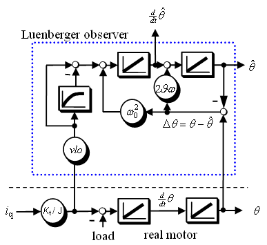
Fig. 5: Luenberger observer based RDC {4}.
Compared with a high resolution (sin/cos) encoder, this configuration has still two major limitations:
accuracy and resolution
The accuracy depends mainly on the specified Resolver performance. Getting more than 8 arc minutes (~ 11.5 bit) accuracy from a Resolver is not the standard.
The resolution depends only on the resolver-to-digital conversion:
- ADC resolution – quantization noise,
- arc tan or sin/cos implementation and
- precision of the digital signal processing.
The resolution limitations are resulting in high bandwidth systems with well audible noise. The noise can be reduced by lowering the tracking loop bandwidth (= filtering) which reduces also the distortion responsiveness of the servo loop.
The advantages of a sampling ADC / software RDC with a Luenberger observer are:
- low additional cost due to available sampling ADC channels and CPU resources.
- low additional PCB-space (analog signal conditioning)
- no motor speed limitations
- configurable bandwidth
- no phase lag due to the Luenberger observer
- sin/cos system gain mismatch compensation
The disadvantages are:
- limited resolution (ADC quantization)
- limited EMI immunity (S&H)
- analog filters for noise reduction
- reference signal phase lag due to the analog filters
Delta Sigma Technology
The new ΔΣ tracking RDC concept is moving as much as possible into the digital domain. Digital filters offer full repeatability. Frequency dependent damping and phase lag will not vary within the production.
Generating an ideal sine reference signal with a ΔΣ modulator does not need many resources. Fig. 6 shows a block diagram of a digital to analog modulator using simple digital circuits. The modulator generates from the 12 bit low sample rate input data an over sampled 1 bit wide bit-stream.
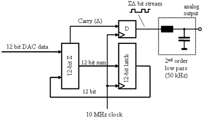
Fig. 6: Simple 12 bit ΔΣ digital-to-analog converter
This bit-stream is generated inside of an FPGA with an update rate of 10 MHz. The desired reference signal carrier frequency is 1250 times lower (8 kHz). On the analog side a simple second order low pass filter with ~100 kHz cut off frequency can remove the harmonics without introducing significant phase lag at the carrier frequency.
The reference sine wave is generated inside the FPGA with an interpolated sin-cos table. Parameters for the sine wave generation block are the amplitude and the phase. These parameters are used to compensate the gain and phase behavior of the (via cable) connected resolver. The result is an analog reference signal with adjustable gain E0 and phase φC and a nearly perfect sine wave, fig. 7.
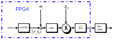
Fig. 7: Schematics of the ΔΣ based sine wave reference signal generation
Looking at a ΔΣ analog to digital conversion there are 3 important design criteria’s:
- ΔΣ modulator order M
- Oversampling ratio OSR
- decimation filter selection
The described ΔΣ based RDC uses the second order modulator (M = 2) ADS 1204 from Texas Instruments {5}, fig 8. The maximum specified sampling clock frequency is fΣΔ = 16 MHz. By choosing an Oversampling Ratio of OSR = 128 we get an ADC update frequency of:
![]() (14)
(14)
This configuration gives us exactly 16 samples per reference sine wave (8 kHz) period.
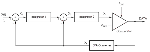
Fig. 8: 2nd order (M = 2) SD modulator {5}
According to fig. 9 the TI modulator ADS1204 provides with an OSR of 128 and a Sinc3 Filter a result with 14 bit precision. Decreasing the OSR to 64 would reduce the precision by two bits to only 12 bit. Increasing the OSR to 256 is not significantly increasing the precision but will double the conversion settling time to 47 µs. Longer settling times are reducing the RDC dynamics.
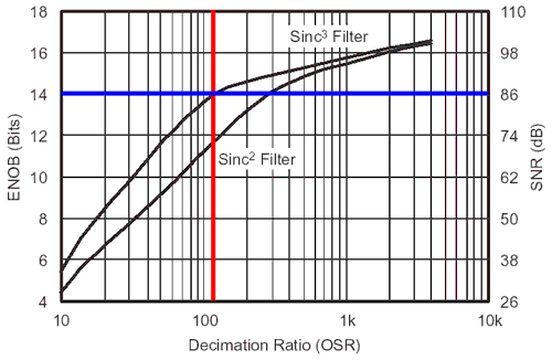
Fig. 9: Effective number of bits versus Oversampling Ratio OSR {5}
The modulator generates only a bit-stream, which is different from a digital word of an analog-to-digital converter (ADC). In order to output a digital word equivalent to the analog input voltage, the bit-stream must be processed by a digital filter. A very simple filter built with minimal effort and hardware is the sinc filter. The frequency response of a third order filter is shown in fig. 11.
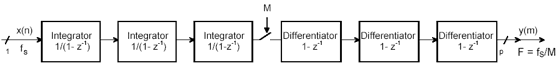
The sinc3 is a very simply structured filter, built with minimal effort and hardware resources, fig. 10.
![]() (15)
(15)
The damping at the carrier frequency is symmetrical (sin cos) and only -0.2 dB.
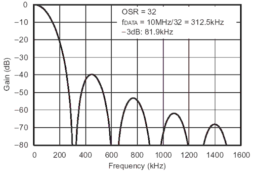
Fig. 11: Frequency response of a sinc3 filter {6}
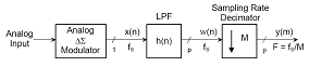
Fig. 12: Schematics of the ΔΣ analog-to-digital conversion system with modulator, digital low pass filter and sample rate decimation
Fig. 12 shows the schematics of the analog-to-digital conversion system. Before building up the tracking loop we should consider some corrections:
- Due to component tolerances there can come up a gain difference between the sine and the cosine channel. To compensate this gain mismatch at least one channel should get a gain correction factor.
- In high bandwidth systems the two converter offsets need to be compensated.
- The cable and Resolver dependent carrier phase lag should be adjusted.
Fig. 13 shows the complete ΔΣ RDC system. The system is running with 3 different update frequencies.
- 10 MHz for the reference generation
- 128 kHz for the ΔΣ ADC result and demodulation
- 16 MHz for the position interpolation

Fig. 13: Block diagram of the new ΔΣ resolver-to-digital converter
Due to the integrating operation principle of the ΔΣ ADCs the EMI immunity is significantly better compared to a sampling ADC. A higher order low pass for the analog signals is no longer necessary. The 8 times higher update frequency compared with the software RDC helps to achieve high bandwidth conversions.
The ΔΣ RDC is tested with a special dual feedback servo motor. A Kollmorgen S300 is running the motor with a sin cos encoder at very low speed. The additional Resolver is connected to a simple laboratory built circuit with the TI ΔΣ modulator and the ΔΣ DAC.
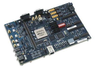
The used FPGA is a Stratix I from Altera on the Altera DSP development board {7}. To show and document the RDC performance a NIOS II soft core CPU was implemented. The ΔΣ RDC system shows more than 16 bit rotor angle resolution by measuring the servo motor at constant speed.
Conclusion
Due to fact that disadvantages of dedicated RDC circuits prevail most modern servo drives are not using dedicated RDC-chips. These drives usually utilize sampling analog to digital converters to demodulate and digitize the Resolver signals. Adding a measured acceleration signal (or the motor current iq) the tracking loop can be extended to a Luenberger observer with no phase lag.
The contribution describes a new FPGA based method to convert the analog Resolver signals to a digital position signal using Delta Sigma technology. By using a 2nd order Delta Sigma modulator it is possible to increase the resolution by 2-bit compared to sampling converters. In a servo drive the significantly better signal to noise ratio can be used to build a smoother motor current (less noisy), or to increase the tracking loop bandwidth. Due to the Delta Sigma modulation the EMI noise from the IGBT Power stage can be suppressed in an efficient way by using digital filters implemented in an FPGA.
With this approach the flexibility of software RDC algorithms are combined with the EMI roughness of a dedicated RDC circuit with no trade-off.
Editors
Prof. Dr.-Ing. Jens Onno Krah
Fachhochschule Köln
Marcel Albers
Fachhochschule Köln
Heiko Schmirgel
Kollmorgen Europe GmbH
Düsseldorf
References
- S300 manual, www.Kollmorgen.com
- 2S82 data sheet, Analog Devices www.analog.com
- J. O. Krah: Software Resolver to Digital Converter for High Performance Servo Drives. PCIM Power Conversion Intelligent Motion, Nürnberg, June 1999,pp. 301-308.
- G. Ellis, J. O. Krah: Observer-Based? Resolver Conversion in Industrial Servo Systems PCIM Power Conversion Intelligent Motion, Nürnberg, 2001, pp. 311-316.
- ADS 1204 data sheet, Texas Instruments www.ti.com
- Combining the ADS1202 with an FPGA Digital Filter for Current Measurement in Motor Control Applications, Texas Instruments application note SBAA0094.
- Altera, www.altera.com